Evolution and Impact of Printed Circuit Boards: A Technological Odyssey
In the realm of electronic innovation, few inventions have been as transformative as the Printed Circuit Board (PCB). These unassuming yet critical components serve as the technological backbone for an expansive array of electronic devices, from our smartphones and laptops to complex aerospace systems. This article explores the fascinating history, construction, and the ever-expanding applications of PCBs, highlighting their indispensable role in our modern world. Check out SMT PCBa to learn more.
A Glimpse into PCB History
The journey of PCBs dates back to the early 20th century, but they truly gained prominence during World War II when the demand for compact and reliable electronic systems soared. Prior to PCBs, electronic connections were made using point-to-point wiring, which was not only time-consuming but also prone to errors and inefficiencies.
1940s - 1950s: Emergence of PCBs
- In the 1940s and 1950s, engineers and innovators began experimenting with the concept of etching conductive pathways onto an insulating substrate, typically made of Bakelite or other materials, to create the first true PCBs.
- These early PCBs used a photoresist and etching process to define the copper traces, laying the foundation for the mass production of electronic devices.
1960s - 1970s: Advancements and Standardization
- The 1960s saw significant advancements in PCB technology, with the introduction of plated through-holes, which allowed for components to be mounted on both sides of the board.
- Standardization efforts, like the development of the IPC-A-600 and IPC-A-610 standards by the Association Connecting Electronics Industries (IPC), played a crucial role in ensuring consistent quality and reliability.
1980s - 1990s: Surface Mount Technology (SMT)
- The advent of Surface Mount Technology (SMT) in the 1980s revolutionized PCB design and assembly. SMT components are smaller and can be placed directly onto the PCB's surface, enabling compact and high-density electronics.
- Multi-layer PCBs with intricate routing capabilities became more common, allowing for more complex electronic systems.
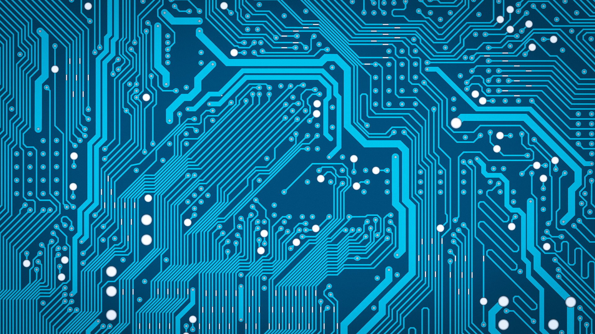
Anatomy of a PCB
A PCB typically consists of several key elements:
Substrate Material
- The substrate, often made of fiberglass-reinforced epoxy (FR-4), serves as the base material. It provides mechanical support and electrical insulation for the PCB.
Copper Traces
- Copper traces are thin conductive pathways that carry electrical signals and power throughout the PCB. These traces are precisely etched onto the substrate.
Components
- Electronic components such as integrated circuits (ICs), resistors, capacitors, and connectors are mounted on the PCB. These components are soldered to the copper traces to establish electrical connections.
Solder Mask
- A solder mask is applied over the PCB to protect the copper traces from environmental factors and prevent unintended solder bridges during assembly.
Silkscreen
- The silkscreen layer includes printed labels, component outlines, and other markings that assist with component placement and identification.
Expanding Horizons: PCB Applications
The versatility of PCBs has led to their integration into an ever-expanding range of applications:
1. Communication Devices
- Smartphones, routers, and communication equipment rely heavily on PCBs to manage wireless communication, data processing, and user interfaces.
2. Healthcare
- PCBs are vital in medical devices such as ECG machines, infusion pumps, and patient monitoring systems, ensuring accurate diagnostics and patient care.
3. Renewable Energy
- In solar panels, wind turbines, and battery management systems, PCBs enable efficient energy conversion and storage.
4. Automotive
- Modern vehicles employ PCBs for engine control, infotainment systems, and advanced driver assistance systems, enhancing safety and performance.
5. Aerospace and Defense
- PCBs are critical in aircraft navigation, communication systems, and missile guidance, where reliability and durability are paramount.
Future Prospects
As we look to the future, PCB technology continues to evolve. Trends such as miniaturization, the adoption of flexible and rigid-flex PCBs, and the integration of advanced materials promise to drive innovation in electronics. PCBs are likely to play an even more central role in the development of emerging technologies, including IoT devices, 5G networks, and artificial intelligence systems.
In conclusion, Printed Circuit Boards have journeyed from their humble origins to become the unsung heroes of the electronics world. Their evolution mirrors the rapid advancement of technology itself, and their versatility ensures they will remain a cornerstone of innovation for years to come. As we navigate an increasingly interconnected and electronic world, PCBs will continue to be instrumental in shaping the future of our digital landscape.